
 English
 中文简体
中文简体 русский
 عربى
عربى Português
 日本語
日本語 한국어
한국어

Advanced ceramics play an indispensable role in semiconductor manufacturing processes (from wafer fabrication to wafer bonding, packaging, and testing) due to their high temperature resistance, corrosion resistance, high hardness, high thermal conductivity, and excellent insulation. As global integrated circuit advanced processes, the harsh operating conditions within equipment pose extreme challenges to the material purity, processing precision, and plasma resistance of key ceramic components. This article aims to address the problem of " vacuum " and lack of parameter correspondence with equipment applications in internal enterprise technical documentation , and to establish core technology internal control standards for all categories of advanced ceramics.
The Four Core Materials of Semiconductor Precision Ceramics
|
Ceramic materials and purity requirements |
Core physical performance indicators |
Corrosion resistance / high temperature resistance limit |
Machining limit tolerance |
Front-end core equipment corresponding |
|
High-purity alumina (Al2O3 ≥ 99.8%) |
Volume resistivity : >10^14 Ω·cm; Hardness : 1800 HV; Elastic modulus : 380 GPa |
Fluorine-based plasma corrosion resistant temperature : 1600℃ |
Flatness : ≤ 2μm ; Roughness : Ra 0.1μm; Minimum aperture : 0.3mm |
Etching machine cavity lining gas spray head vacuum chuck |
|
High thermal conductivity aluminum nitride (AlN ≥ 99%) |
Thermal conductivity : 170-220 W/(m·K) Coefficient of thermal expansion : 4.5×10^-6/K Breakdown voltage : ≥ 15 kV/mm |
High temperature resistance ( withstands rapid heating and cooling ) : 1400℃ |
Parallelism : ≤ 3μm; Internal flow channel accuracy : 0.05mm |
Electrostatic chuck (ESC) CVD heating stage power device substrate |
|
High-solids silicon carbide (SiC, free Si ≤ 0.1%) |
Elastic modulus : 410 GPa; Thermal conductivity : 150 W/(m·K); Mohs hardness : 9.5 |
Resistance to strong acid and alkali vapor phase corrosion : Temperature withstands 1800℃ |
Large-size (>1m) deformation : ≤ 5μm; Mirror surface roughness : Ra 0.02μm |
Etching focusing ring diffusion furnace wafer boat lithography machine workpiece stage skeleton |
|
High-toughness silicon nitride (Si3N4) |
Fracture toughness : 6.5 MPa·m^1/2; Flexural strength : 850 MPa ; Density : 3.2 g/cm3 |
High fatigue and impact resistance; temperature tolerance : 1200℃ |
Fit clearance : 1-2μm; Dynamic balance grade : G1.0 |
High-speed vacuum pump, ceramic bearing, wafer dicing machine spindle, sealing and testing high-frequency fixture |
Performance and control standards of core equipment and key components
- Etching Equipment – Core Consumables System
In the front-end etching process of integrated circuits, whether using ICP (inductively coupled plasma) or CCP (capacitively coupled plasma) equipment, the internal components are exposed to extremely active fluorine-based (such as SF6 , CF4 ) or chlorine-based plasmas. Traditional materials are highly susceptible to chipping due to grain boundary erosion, leading to severe particle contamination of the wafer.
Core product: High-purity silicon carbide focusing ring
[ Image of a silicon carbide (SiC) focusing ring for etching machines ]
- Extreme Plasma Erosion Resistance Technology:This product uses pressureless sintered high-purity silicon carbide with a total metal impurity content ≤ 5ppm . Its unique high-density integrated grain structure results in a chemical etching rate 8-10 times lower than fused silica under strong fluorine-based plasma bombardment . This ensures that the edge step deformation rate of the focusing ring is less than 0.05% during 200 consecutive wafer etching cycles, greatly improving the uniformity of wafer edge etching and increasing the overall machine uptime by more than 15% .
- Precise resistivity doping control:Through advanced grain boundary conductivity modulation technology, the resistivity is stably controlled within the specific range required by the customer ( 1-10 Ω·cm ). Under hundreds of watts of high-frequency radio frequency ( RF ) power, the plasma electric field is guaranteed to penetrate the wafer edge vertically and uniformly, eliminating the etching edge effect.
Core product: High-purity alumina precision spray head
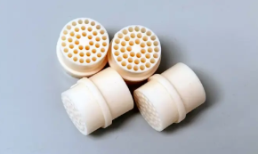
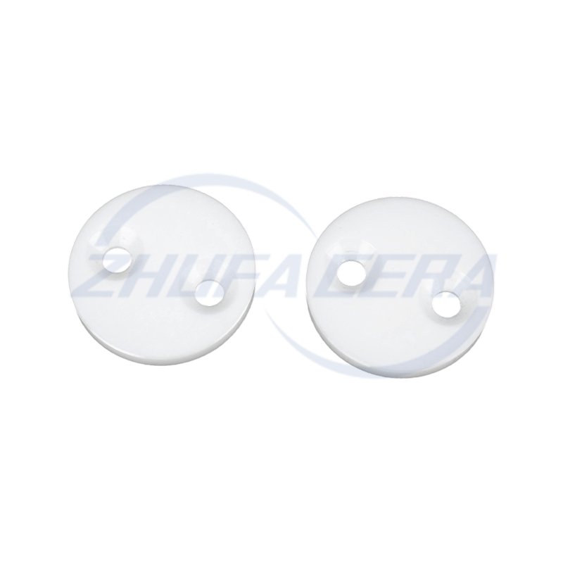
[ Detailed image of micro-porous machining of high-purity alumina ceramic spray head ]
- Ultra-precision micro-hole flow field processing:On a wafer surface with a diameter of 300-450mm , more than 5000 micro-holes with a diameter of 0.3mm-0.5mm are arranged through ultrasonic and five-axis precision CNC linkage machining . The overall hole diameter consistency tolerance must be ≤ ±0.01mm , and the inner wall roughness of the holes must reach Ra ≤ 0.2μm , completely eliminating burrs. The process gases (such as Ar, O2, N2 ) are ensured to be sprayed onto the wafer surface in an absolutely laminar flow state.
- Countermeasures for internal control failures:【Prevention of grain boundary cracking and particle contamination】In response to the problem that traditional alumina parts are prone to microcracks at the edges of micropores due to thermal stress release, this product must be tested by a100% polarized stress meter before leaving the factory. The surface is then subjected to non-destructive chemical pickling and polishing to eliminate residual stress from machining and ensure that no local cleavage chipping occurs during 3000 hours of continuous etching service.
- Thin Film Deposition Equipment ( CVD/PVD Machines) – High Temperature and High Pressure Environment
Chemical vapor deposition ( CVD ) and atomic layer deposition ( ALD ) processes require heating and reacting precursor gases, with ambient temperatures typically between 400°C and 1000°C . The wafer must achieve absolute flatness and rapid, uniform thermal distribution.
Core Product: Aluminum Nitride Precision Electrostatic Chucks
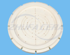
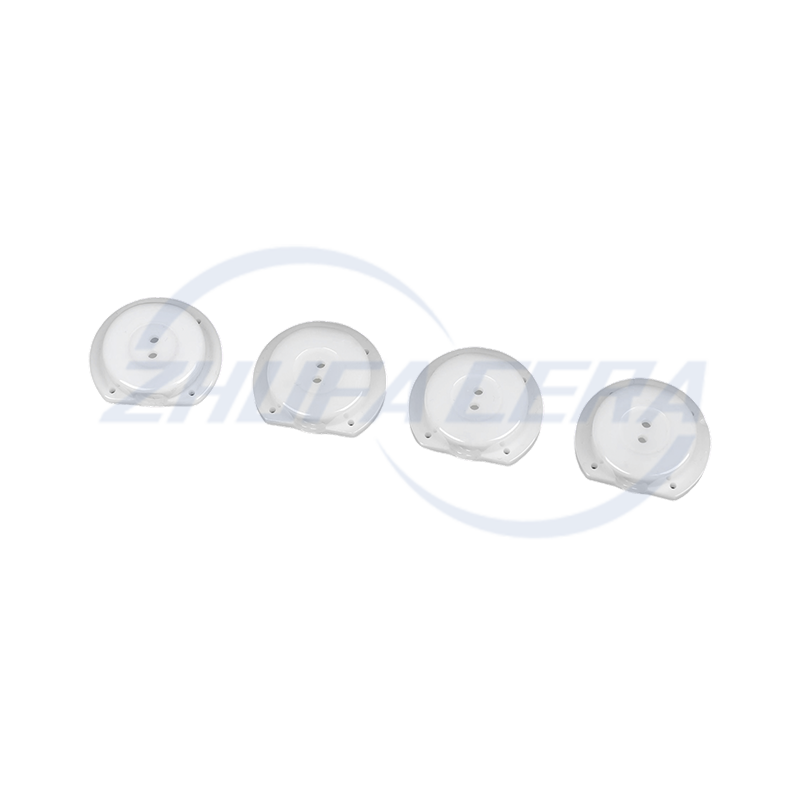
[ Appearance image of aluminum nitride ( AlN) semiconductor electrostatic chuck and heater ]
- Limiting Thermal Conductivity and Thermal Matching Ratio:Aluminum nitride ( AlN ) boasts a high thermal conductivity of 180-220 W/(m·K) , and its coefficient of thermal expansion ( 4.5×10^-6/K ) achieves perfect matching with that of monocrystalline silicon wafers ( 4.2×10^-6/K ) across the entire temperature range of 25℃-800℃ . During rapid high-power heating, it effectively absorbs thermal stress, preventing thermal slip, misalignment, or warping deformation of the silicon wafer , and strictly controlling the temperature field non-uniformity on the wafer surface to ≤ ±0.5℃ .
- High-temperature and high-pressure integrated insulation molding:Utilizing multilayer co-fired ceramic ( HTCC ) technology, high-melting-point tungsten / molybdenum thermoelectric electrodes and electrostatic adsorption electrode patterns are directly printed and embedded within the AlN matrix. Even at 600℃ , the volume resistivity remains ≥10^11 Ω·cm , and the insulation breakdown voltage ≥15 kV/mm , fully meeting both Coulomb force and JR effect adsorption specifications.
Core Product: High-purity silicon carbide wafer carrier for high-temperature furnace tubes
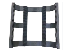
[ Detailed image of the high-purity silicon carbide wafer boat slots for a high-temperature vertical diffusion furnace ]
- High-Temperature Creep Control:In a 1200℃ high-temperature vertical diffusion furnace, traditional quartz boats are prone to high-temperature creep (bending deformation) due to long-term exposure to their own weight and wafer load. This product uses recrystallized / pressureless sintered silicon carbide, which maintains its bending strength without any reduction at an extreme high temperature of 1350℃ . It will not bend or warp during long-term service, ensuring the absolute positional accuracy of automated robotic arms when inserting and removing wafers.
- Wafer Transfer and Automated Handling System – High-Speed, High-Frequency Vibration Damping
With the increase in advanced process capacity, the acceleration of robotic arms handling wafers has reached or even exceeded 2G . Any slight mechanical vibration can cause wafer chipping or back scratches.
Core Product: High-stiffness, large-size silicon carbide robotic arm
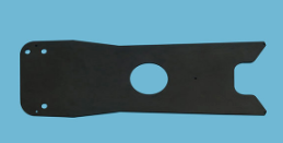
[ Image of a high-vacuum, high-acceleration vacuum handling robotic arm for ceramics ]
- Extremely High Rigidity and Instant Vibration Reduction: Silicon carbide's elastic modulus ( ~410 GPa ) is twice that of steel and six times that of aluminum, and its specific stiffness (elastic modulus / density) is extremely high among engineering materials. The silicon carbide robotic arm, with its hollow, lightweight structure design, reduces structural response delay during high-speed start-up and shutdown by more than 85% compared to traditional metal components , and the end-effector residual vibration time is less than 0.05 seconds. This completely solves the problem of " vibration and scratches " during handling , ensuring high-speed, high-precision transfer of 12- inch ( 300mm ) large-size thin wafers.
- Dimensional stability in large-size machining:For large-size robotic arms with a length exceeding 1000mm , the flatness tolerance is controlled within ≤ 0.02mm throughout the entire length range , and the surface is mirror polished ( Ra ≤ 0.05μm ) without generating any friction-released particles.
Core product: Porous ceramic vacuum suction cup
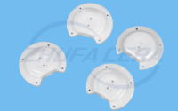
[ Porous Ceramic Vacuum Suction Cup ]
- Uniform porous negative pressure adsorption:The average pore size is controlled at 10-30μm , and the porosity is stable at 35%-45% . Uniform negative pressure is achieved throughout the entire disk through micropores distributed on the surface, avoiding localized stress concentration and localized depression deformation caused by traditional centralized suction cups on thin wafers, and ensuring that the surface remains in a nanometer-level flat state during wafer inspection and CMP polishing.
Summary of material compatibility
- Alumina ceramic precision structural parts series
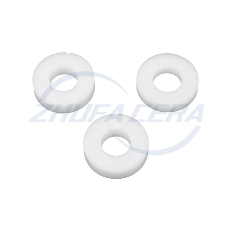
- Key features: High cost-effectiveness, high purity, dust-proof, and strong universal insulation. • Applicable product keywords: Semiconductor ceramic lining, corrosion-resistant insulating ring, high-purity ceramic insulating bushing, ceramic insulating flange.
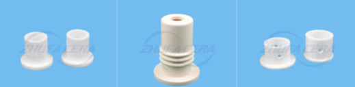
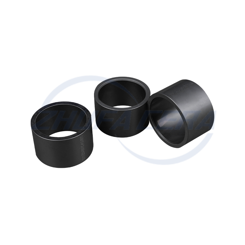
[ Collection of images of various specifications of semiconductor-grade high-purity alumina ceramic structural components ]
- Silicon carbide ceramic reaction
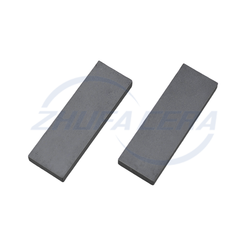
- Key features: Plasma etching resistance, extreme high-temperature resistance without creep, high specific stiffness, large-size one-piece molding. • Applicable product keywords: SiC etching focusing ring, semiconductor silicon carbide cantilever beam, vertical furnace silicon carbide boat, CMP polishing ring, high-rigidity ceramic robotic arm.
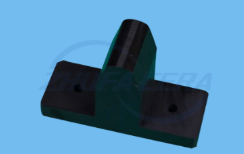
[ Image of high-purity reaction-sintered silicon carbide precision ceramic parts ]
- High thermal conductivity aluminum nitride ceramic /HTCC copper-clad series
- Key features: Ultra-high heat dissipation, thermal expansion coefficient perfectly matched to single-crystal silicon, and multilayer co-fired ( HTCC ) embedded circuit technology. • Applicable product keywords: AlN electrostatic chuck base, semiconductor laser heating element, high-power LED/IGBT ceramic heat sink substrate, metallized aluminum nitride ceramic.
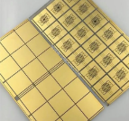
[ Diagram of high thermal conductivity aluminum nitride ceramic substrate and metallized ceramic shell ]
- Ultra-high strength silicon nitride ceramics
- Key features: King of ceramics, high fracture toughness and impact resistance, wear-resistant and dust-free, high-speed rotational dynamic balance. • Applicable product keywords: Vacuum pump ceramic bearings, semiconductor dicing machine ceramic spindles, high-frequency packaging and testing fixtures, wear-resistant ceramic plunger pump cores.
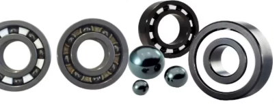
[ Image of high-strength silicon nitride ceramic bearings and wear-resistant components for semiconductor equipment ]